Overview: Wafer laser scribing is a technology that utilizes the high precision and high efficiency of lasers to perform precise scribing operations on the wafer surface.
Principle: The basic principle of laser scribing is that laser pulses are irradiated on the wafer surface, and by controlling the energy, pulse width, frequency, and other parameters of the laser pulses, the physical and chemical reactions on the surface are triggered, thus forming specific lines or patterns on the wafer surface. Specifically, the laser pulse may cause the surface material to melt, evaporate, or decompose, forming specific lines or patterns. These lines or patterns can be precisely controlled and reproducible by controlling parameters such as the repetition rate of the laser pulse, beam quality, and so on.
Through computer control, the laser scribing process can achieve precise line width control and pattern repeatability, which is applicable to the production process in the fields of large-scale integrated circuits, microelectronics, and optoelectronics. By precisely controlling the laser parameters, the scribing accuracy and line quality can be ensured, and production efficiency and product quality can be improved. In addition, wafer laser scribing technology can also be used for wafer surface pretreatment, to improve the accuracy and efficiency of the subsequent processing process.
Application: In semiconductor manufacturing, wafer scribing is one of the crucial steps in the manufacturing process. Through scribing, wafers can be divided into different areas to manufacture different semiconductor devices. The accuracy and quality of scribing directly affect the performance and reliability of semiconductor devices. Laser scribing technology can realize the precise processing and modification of wafer surfaces and improve the accuracy and reliability of scribing by precisely controlling the laser parameters and material parameters.
In the field of microelectronics, wafer scribing can be used to manufacture microelectronic devices with specific lines and component distribution. Through laser scribing technology, the width and spacing of the lines can be precisely controlled, thus realizing efficient and high-precision microelectronics manufacturing.
In the field of optoelectronics, laser scribing technology can be used to manufacture optical devices with specific optical properties, such as gratings, lenses, and so on. Through laser scribing, the size and shape of optical devices can be precisely controlled, thus improving optical performance and reliability.
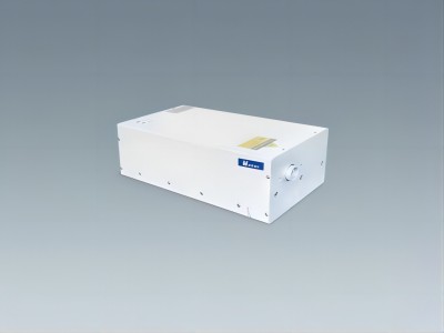
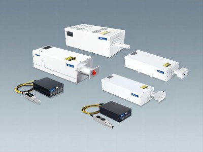
Maiman’s Elite series of high-energy UV lasers bring significant efficiency gains and process simplicity to the silicon carbide (SiC) wafer process. This advanced laser technology makes the scribing process more efficient, reduces the complexity of wafer handling, and minimizes the risk of chip damage during processing. Efficient scribing: Scribing time can be less than 30 minutes for 6-inch silicon carbide wafers, dramatically increasing production throughput.
Efficient scribing: For 6-inch silicon carbide wafers, the scribing time can be less than 30 minutes, significantly improving production throughput.
Extremely low chipping rate: Chipping during the cutting process is less than 2 microns, ensuring cut quality and reducing scrap.
One-step dicing process: Ability to directly cut off metalized wafers without the need for multi-step pre-processing, simplifying the manufacturing process.
Reduced risk of damage: Reduced wafer handling steps reduce the possibility of chip damage during processing.